Introduction
There are two main ways to employ binary diffraction gratings. Typically, binary diffraction grating is used to excite preexisting waveguide. Nowadays, special attention is paid to single-layer high-contrast diffraction structures by virtue of a significant progress in semiconductor technology. To correctly analyze such a type of the structures as continuation of the Modes feature for the modal codes, we elaborated an additional feature for calculating the interference of single-layer binary grating selected modes. Codes are provided along with help that gives a brief description of this feature. The main purpose of this page is to provide a keen user with a more thorough description of the possibilities of the Interference of grating Modes using specific examples.
Introduction (O. Parriaux)
Resonant reflection of an optical wave by a grating waveguide has been known since the mid-eighties [1]. Since then, hundreds of scientific papers have been published. The best known application is in bio sensing where the 100% reflection peak angular or spectral position depends on the bio reaction taking place at the corrugated waveguide surface.
Later on, the development of microelectronic technologies towards smaller nodes has enabled the micro structuring of layers down to a feature size well below the visible and near-IR wavelength. The characteristics of these structures are high refractive index materials such as silicon, and binary corrugations as obtained by anisotropic dry etching, the grooves extending in general all through the etched layer. Although they exhibit the same effects as in lower index contrast structures, specific characteristics have been revealed such as strong intra-guide interactions adjustable by controlling the corrugation duty cycle, highly efficient coupling, and ultra-broad or ultra-narrow resonances. The latter were found when searching for conditions giving rise to resonant reflection at the end face of a single mode optical fiber, i.e., when the finite beam of a fiber core sees few grating periods only [2]. It was assumed and shown at that time that the discovered arbitrarily narrow resonant reflection peak was due to the excitation of a waveguide mode of the grating [3].
Later on, the diffractive optics community investigated such unusual effect on the basis of their own concepts, and it was shown that it can nicely be interpreted as the destructive interference in the transmission medium of two grating modes propagating up and down the grooves and walls of the segmented layer. This was developed simultaneously in Ref. [4] and [5] that also gave the dispersion equation governing the optogeometrical parameters that give rise to such arbitrarily narrow resonance in 1D structures. The team of Chang-Hasnain then extended this grating mode way of seeing to 2D periodic structures [6].
The analysis and design of such high index contrast and deep structures can not easily be given a simple phenomenological representation permitting to solve the inverse problem quasi-mentally, unlike in low contrast shallow structures, thus the need of a tool that can solve the direct and inverse problems numerically and delivering all parameters pertaining to both waveguide and grating mode approaches. This is what the present utility does.
References
- Golubenko G A, Svakhin A S, Sychugov V A and Tishchenko A V "Total reflection of light from a corrugated surface of a dielectric waveguide" Sov. J. Quantum Electron. 15 886-7 (1985) [View]
- E. Bonnet, X. Letartre, A. Cachard, A. V. Tishchenko and O. Parriaux, "High resonant reflection of a confined free space beam by a high contrast segmented waveguide", Opt. Quantum Electron. 35, 1025-1036. (2003) [View]
- E. Bonnet, A. Cachard, A. V. Tishchenko, O. Parriaux, "Scaling rules for the design of a narrow-band grating filter at the focus of a free-space beam", Proc. SPIE 5450, Photonic Crystal Materials and. Nanostructures, (15 September 2004) [View]
- Th. Kämpfe, A.V. Tishchenko, O. Parriaux, "Modal representation and normalized scaling rules for ultra narrow-band reflection from a 1D binary corrugation", 8th EOS Topical Meeting on Diffractive Optics, Feb. 2012, Delft, The Netherland [View]
- V. Karagodsky and C.J. Chang-Hasnain, "Physics of near-wavelength high contrast gratings", Optics Express, Vol. 20, No 10, pp. 10888-10895 (2012) [View]
- B-W Yoo, M. Megens, T. Chan, T. Sun, W. Yang, C.J. Chang-Hasnain, D.A. Horsley, M.C. Wu, "Optical phased array using high contrast gratings for two dimensional beamforming and beamsteering", Optics Express, Vol. 21, No 10, pp. 12238-12248 (2013) [View]
Introductory Provisions
What comes to the proposed examples of structures, all refractive indices meet the requirements of the demonstration versions of codes. Thus, there is no need to license MC Grating codes to check the positions of this page. All the refractive indices do not depend from the wavelength, therefore we can use the normalized parameters Period\Wavelength and (Grating layer thickness)\Wavelength. Hence, a fixed Wavelength of 1000 nm is used throughout all the examples. All files, which are referenced on the page, can be found in the Interference Files archive. We are grateful to Oliver Parriaux (professor emeritus at St-Etienne University) for a fruitful discussion regarding provisions described on this page.
Resonance Phenomena in a High-Contrast Binary Diffraction Grating
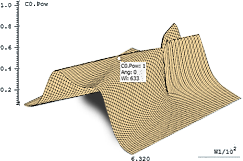
We studied a binary diffraction grating layer, which consisted of equal sections with refractive indices 1 and 3.5, correspondingly. The grating layer was placed on a medium with a refractive index of 1. Figure 1 shows a diagram of normal reflection of radiation from the grating layer incident on it (Per_Thi_Full_Scan.mdl file). As it can be seen from the diagram, the horizontal axis denotes layer's thickness. Since the modes of grating layer do not depend on its thickness, they are calculated just once for all the row points. This reduces calculation time of the diagram by several times. Scanning is performed within a wide range of parameter values with the minimum allowed number of the modes to preserve the diagram and additionally reduce a scanning time.
It can be assumed that resonance does not disappear at any certain point, but its width can decrease, and sharpness of the resonance can subsequently increase. At that, complete reflection is preserved.
Figure 2 shows one of these peculiar sections (Per_Thi_Zoom_Scan.mdl file) in more detail. The scan time for this file is also minimized.
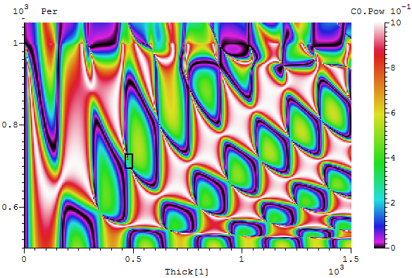
Figure 1. Full scan with selected area of peculiarity being included.
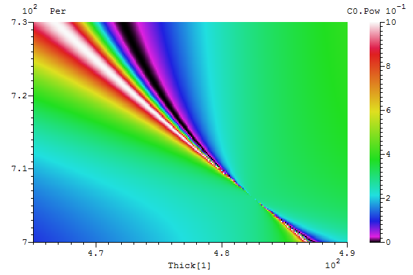
Figure 2. Scaling of the area selected in Figure 1.
Table
Δλ – full width at level 0.7; Δθ – half width at level 0.5; Emax - the maximum value of the Y component of the electric field modulus in the grating layer.
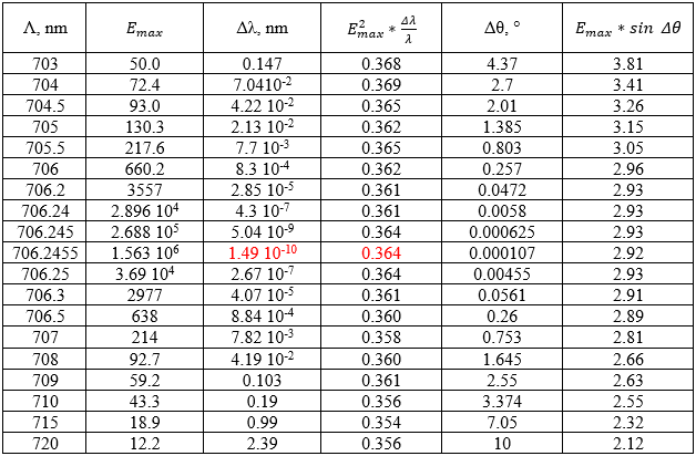
The table shows the results of a detailed study conducted using different values of the period near the singularity of Figure 2. For each period value, thickness of the layer was optimized to maximize reflection of incident radiation along the normal one. Each line in the table corresponds to a demo file with period value being included to its name. 101 modes were used during calculations to ensure adequate outcome.
It should be noted that dependency of exact position of ultra-narrow resonances from such the structure parameters as refractive indices, a wavelength, a period, and a thickness of the layer is very intricate. Unfortunately, MC Grating codes do not allow automatic search of the position of these peculiarities. Therefore, to determine these positions in absence of refractive index dispersion and during allowed duration of the double precision of digits in the codes, you must manually select the period/wavelength or thickness/wavelength value and optimize a thickness or a period of the layer whilst ensuring complete reflection. Then it is necessary to draw the field distribution in the optimized structure. The goal is to obtain the maximum possible field within grating layer. The maximum values of the Y component of the electric field modulus in the grating layer were 1.56 106 and 4.17 106, respectively (Per_706.2455.mdl and Thi_482.4964.mdl files). Greater values could not be obtained. Apparently, this is due to the double precision of digits in the code. From a practical point of view, these values can be considered as infinity. Only Per_706.2455.mdl file is shown in the table. Double accuracy does not allow us to determine so small spectral width of the resonance in this case. Therefore, this value is calculated based on a hypothetical value in the next column, and they both are highlighted in red.
Since the form of field distribution in the grating layer remains unchanged for all the Table files, energy accumulated in the layer is proportional to a square of the maximum value of the Y field component. Constancy of the values in the fourth column of the table corresponds to the fundamental physical principle. The latter principle states that spectral width of the resonance is proportional to energy loss of the resonator related to energy stored in it. Ultra-narrow resonance also has the following feature. Unlike spectral width of the resonance, sixth column of the Table demonstrates that angular width behaves in a completely different way compared to usual one. Typically, spectral and angular widths change quite synchronously in case when grating is used as a weak mean of exciting a planar waveguide.
Probable Nature of Ultra-Narrow Resonance
It is convenient to simplify Figure 1 by selecting appropriate areas with a reflection close to 100% as it is shown in Figure 3.
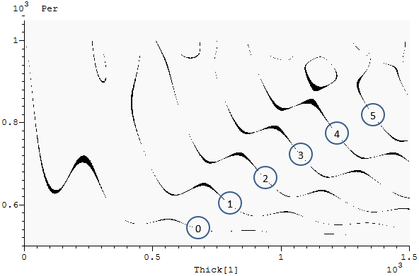
Figure 3. Reflection exceeds 0.999 compared to that in Figure 1. This figure was obtained using specially compiled code.
As it can be seen from this Figure, continuous trajectories disappear in regions with ultra-narrow resonances. Complying with reasonings provided in the previous section, complete reflection is still observed in these "disappearing" regions. Thus, it can be assumed that each continuous trajectory corresponds to excitation of a mode of the same kind. Similar to case with a low-contrast grating layer, one can also assign indices to these trajectories. Zero transmission to the substrate or complete reflection of the grating modes at the interface with the substrate is observed since reflection on the trajectories of the mode excitation is close to complete. Based on reasonings provided in the previous section, ultra-narrow resonance is accompanied by significant accumulation of energy in grating layer. Hence, in addition to complete reflection of the grating modes at the boundary with substrate, reflection of these modes at the boundary with cover should be close to complete. Analysis of interference of the grating modes near ultra-narrow resonances has shown that it is necessary to include evanescent modes of low order in the group of interfering grating modes in addition to propagating modes of 0 and 2 orders to fulfill this condition. For example, files Per_706.2455.mdl or Thi_482.4964.mdl use 101 modes. To provide an adequate description of ultra-narrow reflection and transmission, the minimum set of grating modes for the interference feature is "0 2 3 6 7 10".
If you have 64-bit MC Grating collinear code installed on your computer, we recommend checking this statement by following the instructions below. It is not necessary to own a license. If you have 32-bit code installed on your computer, then you can open the corresponding file such as Per_706.2455.jpg or Thi_482.4964.jpg, containing the graphs obtained on the 64-bit code. Start Modal Collinear code, open one of the above-mentioned files and run it. Scan through the thickness of the layer; draw a black graph with a line thickness of 3 points. Click Settings -> Modes -> Modes Calc -> Interference. Type 0.007 in the selected first line instead of 0.2 or select the second line and type "0 2 3 6 7 10" in it, dividing digits by double spaces. Click Refresh. The program offers 6 TE modes. You can be sure that global indices of these modes are 0, 2, 3, 6, 7 and 10. Click the Graph button, select a yellow color and the line thickness of 1 point and click OK. Black curve will appear in center of the wide resonance as a yellow thin line drawn based on selected modes. Thus, selected modes are sufficient to correctly describe dependence of the reflection on layer's thickness.
Now, we investigate how modules of the selected modes change within the same thickness range. Choose the Grating Mode in Graph Output. Amplitudes greatly increase the unit, so type 0.00001 instead of 1 in the Scale window. Click Graph, select Black color and click OK. In Grating (Local), increase the index to 1, click Graph and select Red, then press OK. Increase the index again and draw a Green graph. Change Scale to 0.01, increase the index to 3 in Grating (Local), click Graph and select Sky color and then press OK. Increase the index again and draw a Blue graph, then increase the index to 5 and draw a Purple graph. You will see that all the six modes including the averaged evanescent one experience a significant resonant increase.
At the end of this section, we study more closely the diagram shown in Figure 1. Details on this subject are found in the following link [View]. In order to prepare these results, we compiled two special codes that give the field distribution of two grating modes of 0th and 2nd orders. Based on these codes, we received very interesting results. A similar approach was used in the work OPTICS LETTERS / Vol. 36, No. 9 / May 1, 2011 [View].
In particular, we found that abnormal reflection (on the marked tracks, Figure 3) is always accompanied by interference of a group of modes. In our symmetric case, when the refractive indices of the cover and the substrate are the same and in the absence of absorption, the amplitudes of the grating modes propagating downward and upward are equal. Thus, the order of the interference of these modes along the z axis is exactly equal to the number of total zeros on the grating period along this axis. On the Period-Thickness diagram, we selected critical points (blue circles correspond to super-narrow resonances and red ones correspond to anti-resonances). Circles are numbered according to the conditional number of the excited mode (track). It turned out that this index exactly coincides with the number of zeros of the 2nd grating mode along the selected points. See the following pictures for the open link. It should also be noted that when moving along the selected track from left to right, the difference of zeros number of the 0th and 2nd grating mode is progressively increased. An additional zero always appears near the cover at the transition point between the blue and red circles. Apparently this does not affect the condition of destructive interference on the side of the substrate preserving abnormal reflection. For blue circles, the difference between the zeros of the 0th and 2nd modes is always even, and for the red ones it is odd. This circumstance determines the essential difference in the behavior of these resonances. With an even difference, the modes phase conditions of the destructive interference on transmission at both boundaries are identical (an ideal condition of high Q resonator for a super-narrow resonance), and for an odd difference, simultaneous destructive interference on transmission at the interfaces with the Cover and the Substrate at the same time is impossible. In the figures, a Super Mode means a complete distribution of the field.
Near-Normal Incidence
Clearly visible narrow tracks of abnormal reflection appear in the reflection diagram (Figure 4) at near-normal angle of incidence on the structure of Figure 1 (Per_Thi_5Deg_Full_Scan.mdl file). For the first time (to the best of our knowledge), such branches of abnormal reflection near the angle of normal incidence on a corrugated planar waveguide were described in Journal of Modern Optics, 1989, Vol. 36, No 11 (I.A. Avrutsky and V.A. Schugov). See Figure 4 adopted from this article. Apparently, this phenomenon has a fundamental nature since it is also observed in the other waveguide structures with diffraction excitation. The interference analysis of grating modes shows that these resonance tracks correspond to a significant resonant increase in the amplitude of the first grating mode. They are accompanied by a relatively weak increase in the amplitudes of the modes 0 and 2 (Per_435.mdl and Per_450.mdl file). It is noteworthy that there is a specific feature of the Y distribution of electric field component present on these tracks. This distribution at any point of track along the X axis corresponds to the first grating mode. However, it has a total number of full period zeros corresponding to the index on the Figure 4 along the Z axis, which denotes the thickness of the grating layer). Please see Figure 5.
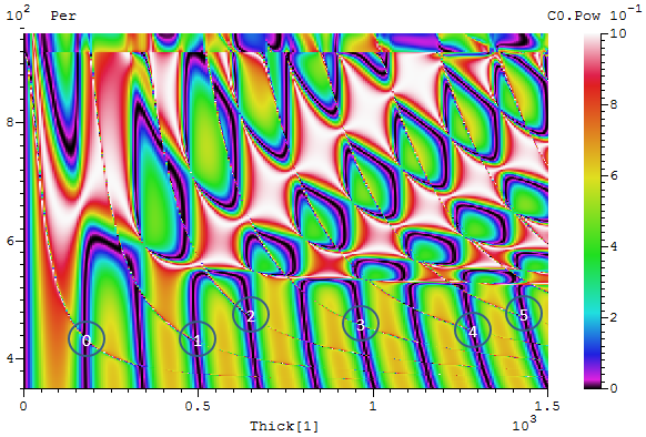
Figure 4. Diagram that resembles Figure 1. The angle of incidence is 5°.
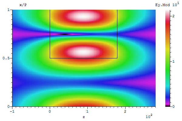
Figure 5. a) - Point 0 (Per_435.mdl file).
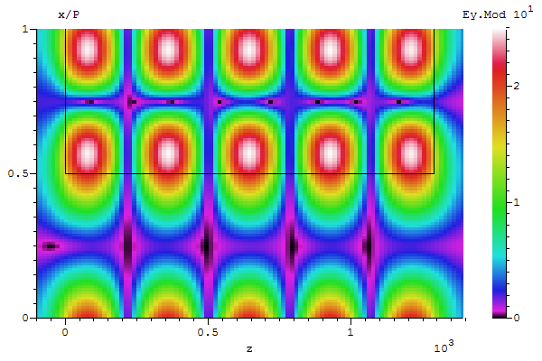
Figure 5. b) - Point 4 of Figure 4 (Per_450.mdl file).
Thus, the principle of indexing these tracks resembles the principle of indexing, which is shown in Figure 3. It is evident that these so-called long-wavelength narrow tracks are likely to correspond to the waveguide modes in Figure 3, complying with the result of the article mentioned in this section. Apparently, the reason for such a significant separation of these trajectories is due to a very strong confluence of the modes of the high-contrast grating propagating along the X axis, and in the opposite direction. The following question arises: why does abnormal reflection of long-wave tracks significantly differ from the one on reflection diagram at the normal incidence? This issue should be addressed separately.
Conclusion
Very interesting results of the interference of grating modes can be obtained by employing an oblique incidence excitation of waveguide modes in single-layered weakly contrasting waveguide structures. However, this study is available only to license holders and is not provided on this page due to the limitations of the demo version.
MC Grating Software is a solution of the diffraction grating analysis and design problems for multilayer periodic 1D and 2D grating structures:
- Multilayer grating filters and mirrors.
- Integrated optics grating couplers.
- Biochemistry sensing chips.
- Wire grid polarizes.
- General multilayer structures.